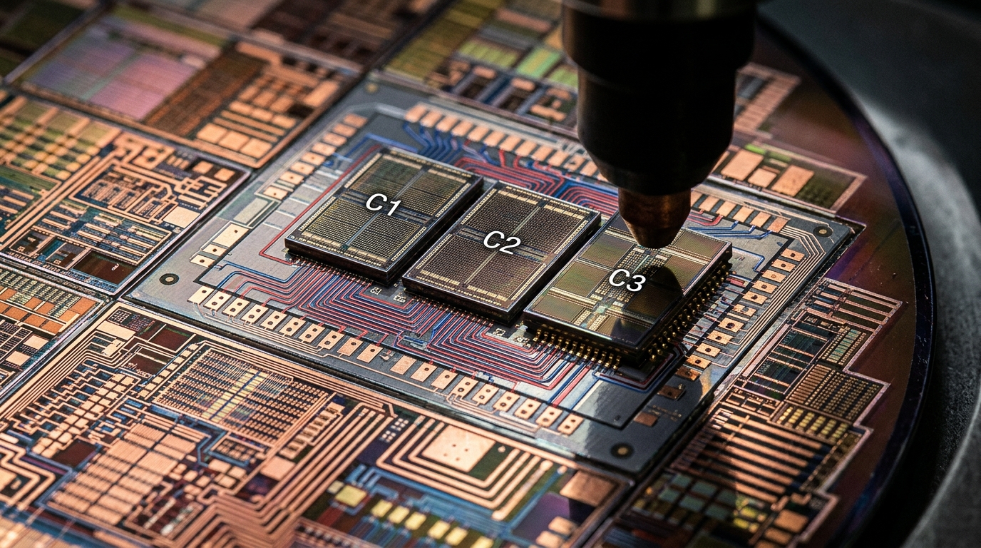
The semiconductor industry is moving through a structural shift. For years, the dominant narrative was that progress meant shrinking transistors on a monolithic chip. In 2026, that story is incomplete. Performance gains are increasingly coming from advanced packaging, modular design, and chiplet architectures.
That change matters because AI workloads are exposing limits in bandwidth, heat management, and cost efficiency. Rather than building ever-larger single dies, companies are splitting designs into smaller specialized components and connecting them through high-performance packaging.
Interconnect technology is now at the heart of the race. Hybrid bonding, standardized chiplet interfaces, and large-scale packaging platforms are becoming essential for next-generation AI accelerators. The goal is not just to make chips faster, but to make them communicate faster with less power loss.
The result is a more distributed semiconductor value chain. Foundries, packaging specialists, and equipment makers are all trying to capture more of the stack. In the AI era, how a chip is assembled may matter almost as much as how it is fabricated.